Researchers at Oregon State University, a Trust grantee, have made news after making strides in intense pulsed light (IPL) sintering. Find the article on OSU’s website here.
Faster production of advanced, flexible electronics is among the potential benefits of a discovery by researchers at Oregon State University’s College of Engineering.
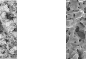
Taking a deeper look at photonic sintering of silver nanoparticle films – the use of intense pulsed light, or IPL, to rapidly fuse functional conductive nanoparticles – scientists uncovered a relationship between film temperature and densification. Densification in IPL increases the density of a nanoparticle thin-film or pattern, with greater density leading to functional improvements such as greater electrical conductivity.
The engineers found a temperature turning point in IPL despite no change in pulsing energy, and discovered that this turning point appears because densification during IPL reduces the nanoparticles’ ability to absorb further energy from the light.
This previously unknown interaction between optical absorption and densification creates a new understanding of why densification levels off after the temperature turning point in IPL, and further enables large-area, high-speed IPL to realize its full potential as a scalable and efficient manufacturing process.
Rajiv Malhotra, assistant professor of mechanical engineering at OSU, and graduate student Shalu Bansal conducted the research. The results were recently published in Nanotechnology.
“For some applications we want to have maximum density possible,” Malhotra said. “For some we don’t. Thus, it becomes important to control the densification of the material. Since densification in IPL depends significantly on the temperature, it is important to understand and control temperature evolution during the process. This research can lead to much better process control and equipment design in IPL.”
Intense pulsed light sintering allows for faster densification – in a matter of seconds – over larger areas compared to conventional sintering processes such as oven-based and laser-based. IPL can potentially be used to sinter nanoparticles for applications in printed electronics, solar cells, gas sensing and photocatalysis.
Earlier research showed that nanoparticle densification begins above a critical optical fluence per pulse but that it does not change significantly beyond a certain number of pulses.
This OSU study explains why, for a constant fluence, there is a critical number of pulses beyond which the densification levels off.
“The leveling off in density occurs even though there’s been no change in the optical energy and even though densification is not complete,” Malhotra said. “It occurs because of the temperature history of the nanoparticle film, i.e. the temperature turning point. The combination of fluence and pulses needs to be carefully considered to make sure you get the film density you want.”
A smaller number of high-fluence pulses quickly produces high density. For greater density control, a larger number of low-fluence pulses is required.
“We were sintering in around 20 seconds with a maximum temperature of around 250 degrees Celsius in this work,” Malhotra. “More recent work we have done can sinter within less than two seconds and at much lower temperatures, down to around 120 degrees Celsius. Lower temperature is critical to flexible electronics manufacturing. To lower costs, we want to print these flexible electronics on substrates like paper and plastic, which would burn or melt at higher temperatures. By using IPL, we should be able to create production processes that are both faster and cheaper, without a loss in product quality.”
Products that could evolve from the research, Malhotra said, are radiofrequency identification tags, a wide range of flexible electronics, wearable biomedical sensors, and sensing devices for environmental applications.
The advance in IPL resulted from a four-year, $1.5 million National Science Foundation Scalable Nanomanufacturing Grant in collaboration with OSU researchers Chih-hung Chang, Alan Wang and Greg Herman. The grant focuses on overcoming scientific barriers to industry-level nanomanufacturing. Support also came from the Murdock Charitable Trust and the Oregon Nanoscience and Microtechnologies Institute.
About the OSU College of Engineering: The OSU College of Engineering is among the nation’s largest and most productive engineering programs. Since 1999, the college has more than tripled its research expenditures to $37.2 million by emphasizing highly collaborative research that solves global problems. It is a leader in signature research areas, including precision health, clean energy, resilient infrastructure and advanced manufacturing; and targeted strategic areas, including robotics, materials research and clean water.
The post Advance in Intense Pulsed Light Sintering Opens Door to Improved Electronics Manufacturing appeared first on M. J. Murdock Charitable Trust.


